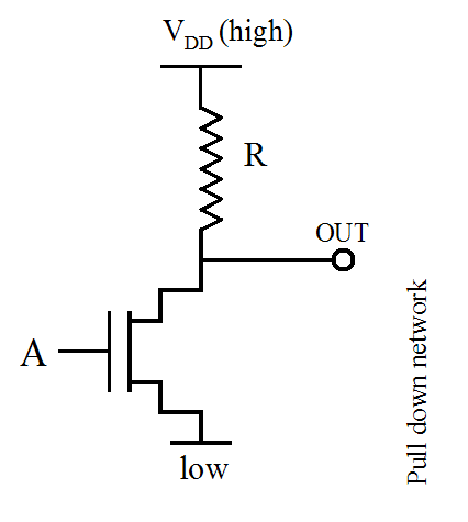
nmos schematic diagram
Activity: CMOS Logic Circuits, Transmission Gate XOR [Analog Devices Wiki]. 9 Images about Activity: CMOS Logic Circuits, Transmission Gate XOR [Analog Devices Wiki] : Digital Logic NOR Gate(Universal Gate) - All About Engineering, Schematic diagram of the conventional two-stage ESD protection circuit and also Download Power On Delay Circuit Diagram Background // Best Diagram Images.
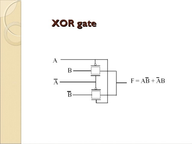
Activity: CMOS Logic Circuits, Transmission Gate XOR [Analog Devices Wiki]
![Activity: CMOS Logic Circuits, Transmission Gate XOR [Analog Devices Wiki]](http://wiki.analog.com/_media/university/courses/electronics/axor_f3.png?w=600&tok=9ea7be) wiki.analog.com
wiki.analog.com
gate xor cmos transmission xnor logic analog exclusive wiki circuits activity figure electronics courses university
Pass Transistor Logic
 www.slideshare.net
transistor gate nmos xor
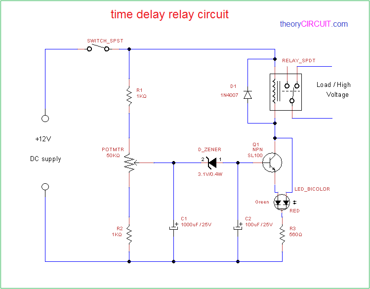
Download Power On Delay Circuit Diagram Background // Best Diagram Images
 diagramjrx.netlify.app
delay 25v theorycircuit 100uf
SATISH KASHYAP: MICROWIND Tutorial Part 5 : Three (3) Input NAND Gate
 satish-kashyap.blogspot.com
input microwind gate nand diagram tutorial three
IC Reverse Engineering And Other Adventures: A Simple Experiment With
 uvicrec.blogspot.com
inverter nmos reverse ic engineering adventures open
Lect5_Stick_diagram_layout_rules
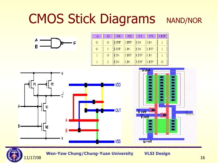 www.slideshare.net
cmos gate nand lect5 schematic
Schematic Diagram Of The Conventional Two-stage ESD Protection Circuit
 www.researchgate.net
esd cmos
Power Supply For Amplifier Archives - Amplifier Circuit Design
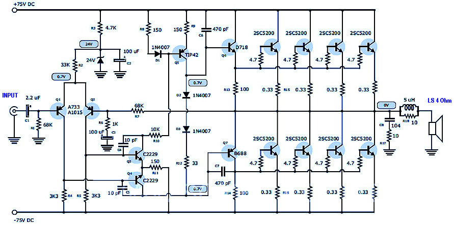 amplifiercircuit.net
amplifier power watt circuit volt transistor schematic pcb audio amplifiercircuit layout supply diagram 400w using output 70v circuits google electronic
Digital Logic NOR Gate(Universal Gate) - All About Engineering
 allabouteng.com
nmos schematic
Cmos gate nand lect5 schematic. Schematic diagram of the conventional two-stage esd protection circuit. Amplifier power watt circuit volt transistor schematic pcb audio amplifiercircuit layout supply diagram 400w using output 70v circuits google electronic